- 您现在的位置:买卖IC网 > Sheet目录1995 > DSD1792DB (Texas Instruments)IC 24BIT STEREO AUD DAC 28-SSOP
DSD1792
SLES067B MARCH 2003 REVISED NOVEMBER 2006
www.ti.com
15
SYSTEM CLOCK AND RESET FUNCTIONS
System Clock Input
The DSD1792 requires a system clock for operating the digital interpolation filters and advanced segment DAC modulators.
The system clock is applied at the SCK input (pin 7). The DSD1792 has a system clock detection circuit that automatically
senses if the system clock is operating between 128 fS and 768 fS. Table 1 shows examples of system clock frequencies
for common audio sampling rates. If the oversampling rate of the delta-sigma modulator is selected as 128 fS, the system
clock frequency is over 256 fS.
Figure 24 shows the timing requirements for the system clock input. For optimal performance, it is important to use a clock
source with low phase jitter and noise. One of the Texas Instruments’ PLL1700 family of multiclock generators is an
excellent choice for providing the DSD1792 system clock.
Table 1. System Clock Rates for Common Audio Sampling Frequencies
SAMPLING FREQUENCY
SYSTEM CLOCK FREQUENCY (fSCK) (MHz)
SAMPLING FREQUENCY
128 fS
192 fS
256 fS
384 fS
512 fS
768 fS
32 kHz
4.096
6.144
8.192
12.288
16.384
24.576
44.1 kHz
5.6488
8.4672
11.2896
16.9344
22.5792
33.8688
48 kHz
6.144
9.216
12.288
18.432
24.576
36.864
96 kHz
12.288
18.432
24.576
36.864
49.152
73.728
192 kHz
24.576
36.864
49.152
73.728
(1)
(1) This system clock rate is not supported for the given sampling frequency.
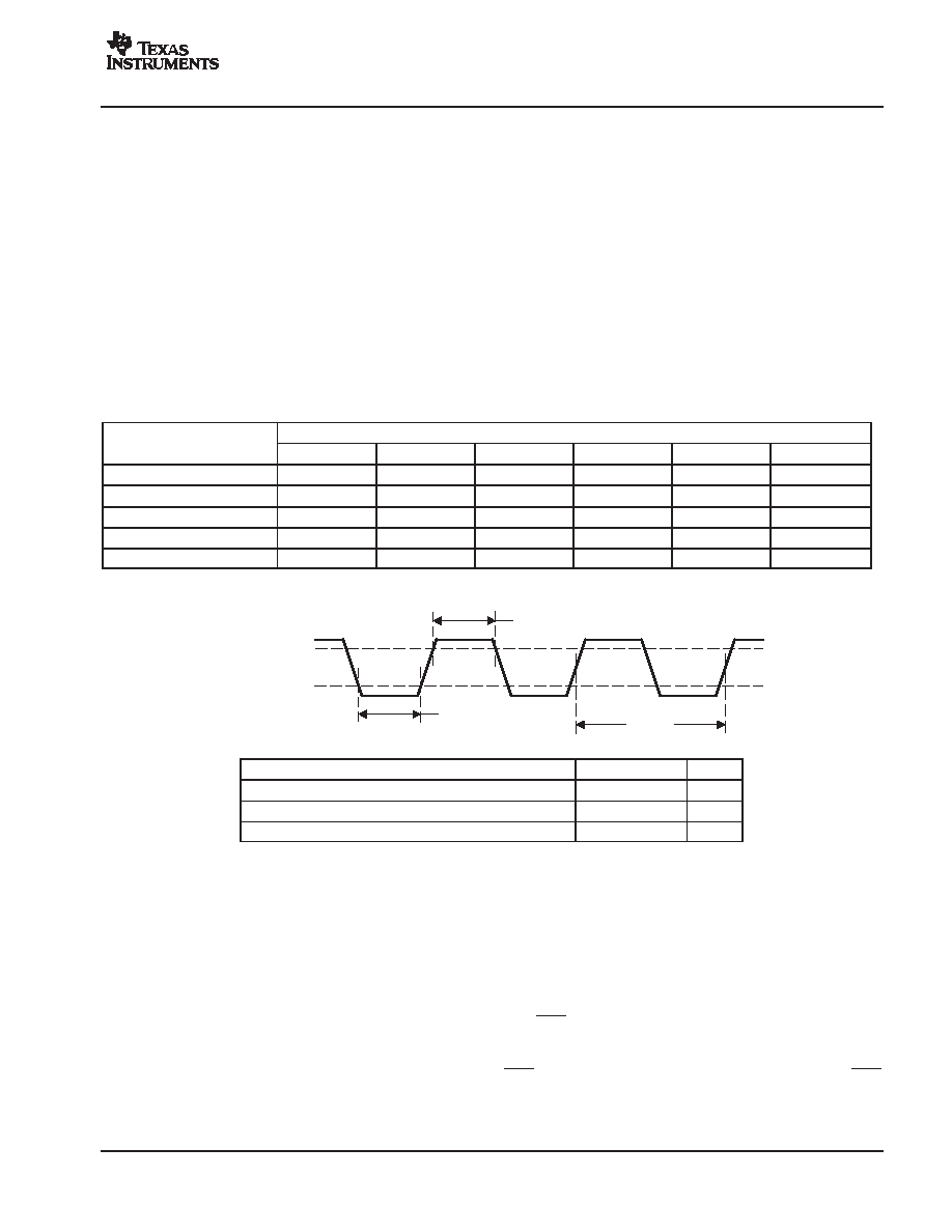
t(SCKH)
t(SCY)
System Clock (SCK)
t(SCKL)
2 V
0.8 V
H
L
PARAMETERS
MIN
MAX
UNITS
t(SCY)
System clock pulse cycle time
13
ns
t(SCKH) System clock pulse duration, HIGH
0.4t(SCY)
ns
t(SCKL) System clock pulse duration, LOW
0.4t(SCY)
ns
Figure 24. System Clock Input Timing
Power-On and External Reset Functions
The DSD1792 includes a power-on reset function. Figure 25 shows the operation of this function. With VDD > 2 V, the
power-on reset function is enabled. The initialization sequence requires 1024 system clocks from the time
VDD > 2 V. After the initialization period, the DSD1792 is set to its default reset state, as described in the MODE CONTROL
REGISTERS section of this data sheet.
The DSD1792 also includes an external reset capability using the RST input (pin 14). This allows an external controller
or master reset circuit to force the DSD1792 to initialize to its default reset state.
Figure 26 shows the external reset operation and timing. The RSTpin is set to logic 0 for a minimum of 20 ns. The RST
pin is then set to a logic 1 state, thus starting the initialization sequence, which requires 1024 system clock periods.
Operation of the external reset is the same as that of the power-on reset. The external reset is especially useful in
applications where there is a delay between the DSD1792 power up and system clock activation.
发布紧急采购,3分钟左右您将得到回复。
相关PDF资料
EL5001IRE-T7
IC CLOCK DRIVER 6-CHAN 20-HTSSOP
FT10001L6X
IC RESET TIMER 6-MICROPAK
FT3001MPX
IC RESET TIMER 8-MLP
FT7521L6X
IC RESET TIMER 7.5SEC 6MICROPAK
FT7522L6X
IC RESET TIMER 6-MICROPAK
FT8010UMX
IC RESET TIMER CONF DELAY 10UMLP
FTS125-COO-010.0M
IC GPS BASED TIMING MOD (OCXO)
FTS125-CTV-010.0M
IC GPS BASED TIMING MOD (TCXO)
相关代理商/技术参数
DSD1792DBG4
功能描述:音频数/模转换器 IC 24-Bit 192kHz Smplng Adv Stg Stereo DAC RoHS:否 制造商:Texas Instruments 转换器数量: 分辨率:16 bit 接口类型:I2S, UBS 转换速率: 信噪比:98 dB 工作电源电压:5 V DAC 输出端数量:2 工作温度范围:- 25 C to + 85 C 电源电流:23 mA 安装风格:SMD/SMT 封装 / 箱体:TQFP-32 封装:Reel
DSD1792DBR
功能描述:音频数/模转换器 IC 24-Bit 192kHz Smplng Adv Stg Stereo DAC RoHS:否 制造商:Texas Instruments 转换器数量: 分辨率:16 bit 接口类型:I2S, UBS 转换速率: 信噪比:98 dB 工作电源电压:5 V DAC 输出端数量:2 工作温度范围:- 25 C to + 85 C 电源电流:23 mA 安装风格:SMD/SMT 封装 / 箱体:TQFP-32 封装:Reel
DSD1792DBRG4
功能描述:音频数/模转换器 IC 24B 192kHz Sampl Adv Segment Aud St DAC RoHS:否 制造商:Texas Instruments 转换器数量: 分辨率:16 bit 接口类型:I2S, UBS 转换速率: 信噪比:98 dB 工作电源电压:5 V DAC 输出端数量:2 工作温度范围:- 25 C to + 85 C 电源电流:23 mA 安装风格:SMD/SMT 封装 / 箱体:TQFP-32 封装:Reel
DSD1793
制造商:BB 制造商全称:BB 功能描述:24 BIT 192 KHZ SAMPLING ADVANCED SEGMENT AUDIO STEREO DIGITAL TO ANALOG CONVERTER
DSD1793DB
功能描述:音频数/模转换器 IC 24-Bit 192kHz Smplng Adv Stg Stereo DAC RoHS:否 制造商:Texas Instruments 转换器数量: 分辨率:16 bit 接口类型:I2S, UBS 转换速率: 信噪比:98 dB 工作电源电压:5 V DAC 输出端数量:2 工作温度范围:- 25 C to + 85 C 电源电流:23 mA 安装风格:SMD/SMT 封装 / 箱体:TQFP-32 封装:Reel
DSD1793DBG4
功能描述:音频数/模转换器 IC 24B 192kHz Sampl Adv Segment Aud St DAC RoHS:否 制造商:Texas Instruments 转换器数量: 分辨率:16 bit 接口类型:I2S, UBS 转换速率: 信噪比:98 dB 工作电源电压:5 V DAC 输出端数量:2 工作温度范围:- 25 C to + 85 C 电源电流:23 mA 安装风格:SMD/SMT 封装 / 箱体:TQFP-32 封装:Reel
DSD1793DBR
功能描述:音频数/模转换器 IC 24-Bit 192kHz Smplng Adv Stg Stereo DAC RoHS:否 制造商:Texas Instruments 转换器数量: 分辨率:16 bit 接口类型:I2S, UBS 转换速率: 信噪比:98 dB 工作电源电压:5 V DAC 输出端数量:2 工作温度范围:- 25 C to + 85 C 电源电流:23 mA 安装风格:SMD/SMT 封装 / 箱体:TQFP-32 封装:Reel
DSD1793DBRG4
功能描述:音频数/模转换器 IC 24-Bit 192kHz Smplng Adv Stg Stereo DAC RoHS:否 制造商:Texas Instruments 转换器数量: 分辨率:16 bit 接口类型:I2S, UBS 转换速率: 信噪比:98 dB 工作电源电压:5 V DAC 输出端数量:2 工作温度范围:- 25 C to + 85 C 电源电流:23 mA 安装风格:SMD/SMT 封装 / 箱体:TQFP-32 封装:Reel